2026-03-12 17:20:23
Обработка на пластини: Основната задача на този процес е да се изработят схеми и електронни компоненти (като транзистори, кондензатори, логически превключватели и др.) върху пластината. Процедурата на обработка обикновено е свързана с вида на продукта и използваната технология, но основните стъпки са първо да се почисти пластината по подходящ начин, след това да се окисли и химически да се отложи върху повърхността чрез пари, а след това да се извършат повтарящи се стъпки като нанасяне на покритие, експониране, проявяване, ецване, йонна имплантация, метално разпрашване и др. Накрая върху пластината се обработват и изработват няколко слоя схеми и компоненти.
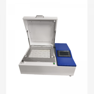
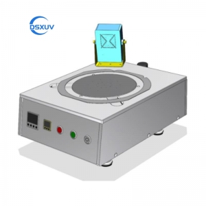
Размерът на пластините обикновено се разделя на: 4-инчови, 6-инчови, 8-инчови, 12-инчови. За да предпазим пластината от надраскване, трябва да използваме монтиране на пластини машина . Нашата машина за монтиране на пластини е заменила патронника с черна антистатична тава, а височината на патронника може да се регулира, за да побере пластини с дебелина от 150 до 700 μm.
Ръчно
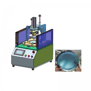
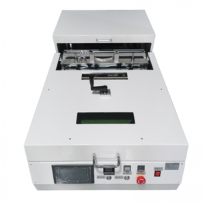
машина за ламиниране на вафли
,
Полуавтоматична вафла
ламинаторна машина
,
Напълно автоматична машина за ламиниране на вафли
.


 български
 English
 français
 Deutsch
 русский
 italiano
 español
 Nederlands
 العربية
 svenska
 +8618924372460
 live:1651063690jennifer
 uvcure@uvspacelight.com
 0086-18924372460